Liz Stevens, writer, UV Solutions
Clean and safe water, long regarded as an infinite natural resource, lately has been recognized for what it really is – a finite, extremely valuable commodity. Gauging the quality of water and examining it for contaminants often require sample collection in the field, followed by transportation to laboratories for time-consuming analysis with expensive technologies. Fariborz Taghipour, professor, Chemical and Biological Engineering, University of British Columbia, and Muersha Wusiman, former graduate student under Professor Taghipour, thought that there must be an easier, faster, less expensive way to analyze water quality for contaminants, and a way to do it on-site. The researchers reimagined the typical fluid-based, laboratory-dependent methodology as a solid-phase, compact and portable technique. In their 2023 IUVA World Congress presentation, “UV LED Activated Sensors for the Detection of Chemical Contaminants in Water,” Taghipour and Wusiman introduced the result of their efforts to combine UV LEDs, nanocrystals, molecularly imprinted polymers and portable spectrometers into one system for water contamination analysis – a water analysis lab-on-a-chip. UV Solutions talked with Professor Taghipour to learn more about this new water-analysis method.
Technology in a Nutshell
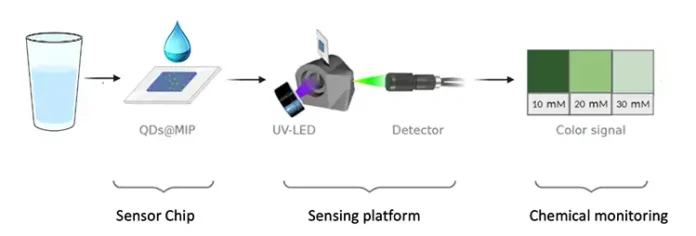
“We have created a lab-on-a-chip optoelectronic sensor for measuring targeted chemicals and contaminants found in a liquid (water),” said Taghipour. “The elements in our technology include a sensing unit housing with a slot for a water-sample testing chip and a UV LED to activate the testing chip, which attaches to a portable spectrometer (Image 1).

“A testing chip can contain one or more sensing nodes,” Taghipour explained, “with each node calibrated to detect a particular contaminant. The sensing nodes are made of fluorescent quantum dots (QDs) and synthetic receptor molecularly imprinted polymers (MIPs).” Quantum dots are semiconductor particles that fluoresce in a predictable way. A molecularly imprinted polymer (MIP) is a polymer that can be produced to contain the molecular shape of a chosen substance – in this case, a contaminant – hollowed out as infinitesimal cavities within the polymer. When quantum dots are mixed with the MIPs and then applied to coat a substrate, the surface of the substrate features a solid layer made of quantum dots that will fluoresce and that possesses empty MIP cavities.
When a water sample is placed on the testing chip and allowed to dry, only the contaminant molecules of the type for which the chip was calibrated will bind to the MIP cavities in the chip. “When excited by the UV LED radiation,” said Taghipour, “the QDs on the chip will generate colorful fluorescent light, the intensity of which is dependent on the chemical environment. Any bound contaminant molecules reduce the fluorescent intensity from the chip, creating a measurable light signal that is related to the contaminant concentration.”
The user can insert a prepared and dried water sample chip into the detector unit, aim a UV LED lamp (at 310 nm for this study) at it and measure the reflected fluorescence with a portable spectrometer (in this study, the USB2000+ Miniature Fiber Optic Spectrometer). The intensity of the reflected fluorescent light then can be used to confirm the presence and estimate the concentration of the contaminant in the water sample. “The more contaminant molecules there are, the more quenching will take place, and the more measurable change there will be in the resulting fluorescent color,” said Taghipour.
Blazing a New Trail
Taghipour and Wusiman used the elements and methods described to create a novel next-generation methodology to overcome drawbacks of various methods and technologies, and to advance water-contaminant analysis.
As Taghipour described the scenario, “Sensors that utilize fluorescence signals of quantum dots and synthetic receptors, such as molecularly imprinted polymer, can provide sensitivity, selectivity and stability to the sensing process. However, there were three main issues associated with the existing QDs@MIP-based sensors.” The first issue was that most of the reported QDs-based sensors typically utilize toxic cadmium-based QDs that harm the environment. For environmental safety, Taghipour and Wusiman switched to a non-toxic ZnO (zinc oxide) material for the quantum dots.
The second issue was the lack of a sample immobilization method: Most of the existing detection processes called for a water sample in the non-portable liquid phase. The researchers created a solid-phase water sample technique by coating a chip with quantum dots and MIPs via spin coating. “Spin coating is a method of creating thin films on a solid substrate and often is used to immobilize sensing materials when devising electrical sensors,” said Taghipour. “Unlike the more prevalent covalent binding method, spin coating does not require functionalization, which makes it a widely applicable, simple and time-efficient alternative. To the best of our knowledge, spin coating has not previously been applied to develop solid fluorescence sensors, despite its advantages.” A water sample then can be applied to the chip and allowed to dry, leaving behind only the contaminants from the water on a dry, immobilized water-analysis chip.
Finally, there are few, if any, studies that use the target-flexibility of MIPs to detect multiple target contaminants at the same time. “The testing chip that we designed can contain multiple sensing nodes, each for the detection of a different contaminant,” Taghipour explained. “The spectrometer can analyze the fluorescence intensity for each designated sensing node, tailored for various contaminants. With the assistance of an accompanying app, we can estimate the concentration of these contaminants.”
Technical Details
“For this study,” said Taghipour, “biologically and environmentally compatible ZnO QDs formed the sensing unit and MIPs that were prepared with the monomer 3-aminopropyltriethoxysilane (APTES), the target template molecule (e.g., 2,4-D or MCLR) and cross-linking agent tetraethyl orthosilicate (TEOS) were the selective recognition elements.” The liquid-phase fluorescence material was immobilized on a substrate via coating methods to produce solid, dry sensing chips. “The contaminants 2,4-D (an herbicide) and MCLR (an algae toxin) were selected as the model target molecules for evaluating the sensor platform,” Taghipour explained. “These target molecules were selected to represent water contaminants with different structures and origins: 2,4-D represented small-sized synthetic molecules, and MCLR represented large biomolecules.” The sensor and the sensing concept first were optimized for measuring 2,4-D, and their advantages were demonstrated. The sensor then was adapted to measure MCLR, demonstrating the sensing platform’s versatility in measuring different target molecules. The MCLR sensor also was tested with spiked tap water samples to evaluate the real-world applicability of the sensor. “The results,” said Taghipour, “showed that the developed sensor was capable of detecting water contaminants with high sensitivity and selectivity, which opens up new opportunities for portable fluorescence sensor development.”
Taghipour summed up the results. “With this work, we are excited to provide a straightforward technique to obtain QDs-based fluorescence sensing chips,” he said. “This application was made possible by our comprehensive study of various immobilization techniques, and optimization of the sensing material and its synthesis technique. Developing reliable QD@MIP sensing nodes will allow solid-phase fluorescence sensors to flourish in ways that overcome the shortcomings of liquid sensors.” Taghipour said that the combination of sensor chips and a handheld battery-operated detector can bring fluorescence sensors one step closer to realization for lab-on-a-chip devices.
Work is underway to enhance the functionality of target sensor nodes, enabling them to emit fluorescence radiation easily detectable by cellphone cameras. “Our aim is to design a compact sensor unit that seamlessly attaches to a cellphone, coupled with the development of a smartphone app for detection of water contaminants. Leveraging the ubiquitous presence of smartphones – equipped with sophisticated image sensors, cameras and processing capabilities – can revolutionize the landscape of environmental monitoring; this represents our future trajectory,” said Taghipour. “We welcome partnerships with sensor and biosensor companies, along with UV LED companies seeking innovative applications for their products”
For more info, visit https://chbe.ubc.ca/fariborz-taghipour/.


